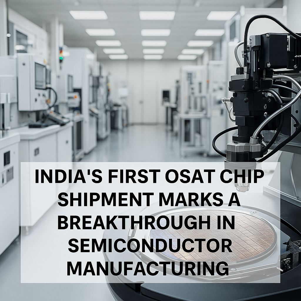
India’s semiconductor story has moved beyond policy intent and pilot ambition into visible manufacturing execution. When Kaynes Semicon shipped India’s first commercially manufactured multi chip Intelligent Power Modules from its Sanand OSAT facility on 15 October 2025, it marked the country’s first export-grade commercial packaging milestone under the India Semiconductor Mission. Since then, the story has advanced further. On 31 March 2026, the Kaynes Semicon facility at Sanand was formally inaugurated, signalling the next phase in India’s semiconductor manufacturing journey.
This progression matters because the October 2025 shipment demonstrated that India could assemble, test, quality-clear, and export sophisticated semiconductor modules for a global customer, while the March 2026 milestone showed that this was not merely a one-time proof point but part of an operational production trajectory. Seen together, these developments strengthen the case that India is moving from semiconductor ambition to semiconductor execution.
India Semiconductor Mission OSAT: The Engine Behind the Breakthrough
The Kaynes Semicon unit at Sanand, Gujarat, was approved by the Union Cabinet on 2 September 2024 under the India Semiconductor Mission. The approved project involved an investment of ₹3,300 crore and was designed for a capacity of 60 lakh chips per day. The project was positioned to serve a wide range of applications including industrial systems, automotive, electric vehicles, consumer electronics, telecom, and mobile devices.
This timeline is important. The project moved from Cabinet approval in September 2024 to India’s first commercially manufactured multi chip module shipment in October 2025, and then to formal inauguration in March 2026. That sequence is far more meaningful than a single shipment headline because it signals real industrial execution rather than an isolated symbolic event.
What Are Intelligent Power Modules (IPMs) and Why Do They Matter?
An Intelligent Power Module (IPM) is a highly integrated semiconductor device that consolidates power switching elements, such as insulated gate bipolar transistors (IGBTs), alongside control and protection circuitry into a single compact chip. These modules are used in a wide array of modern technologies, especially in:
- Electric Vehicles (EVs)
- Renewable energy systems
- Motor control applications
- Industrial automation
This particular IPM is not an ordinary chip, it contains 17 dies inside, including:
- 6 IGBTs
- 2 controller integrated circuits (ICs)
- 6 fast recovery diodes (FRDs)
- 3 standard diodes
This level of integration places the module among the most advanced in its class, and according to Raghu Panicker, CEO of Kaynes Semicon, it is a rare and highly sophisticated achievement. “Companies generally think of doing single-die packaging. We delivered a multi-chip module,” Panicker said, speaking to The Economic Times.
What Changed after the First Shipment?
The October 2025 dispatch of 900 Intelligent Power Modules to Alpha & Omega Semiconductor was the first commercial proof that the Sanand facility could execute assembly, testing, and quality clearance for a global semiconductor customer. Kaynes disclosed that the Sanand OSAT is designed to reach 6.3 million chips per day once fully operational, and described the October shipment as the start of commercial production for AOS, with further ramp-up planned thereafter.
The next important milestone came on 31 March 2026, when the Prime Minister inaugurated the Kaynes Semicon facility. At that stage, the public narrative was no longer about whether India could produce an export-grade semiconductor module once. It had moved to the larger question of whether India could build credible, repeatable semiconductor manufacturing capability under the India Semiconductor Mission.
Why This Matters to India’s Chipmaking Aspirations
For years, India’s strength in semiconductors lay more in chip design, embedded systems, and engineering services than in high-value manufacturing stages such as assembly, packaging, and testing. The Sanand milestones matter because they narrow that gap in a visible and commercially relevant way. First came project approval. Then came India’s first commercially manufactured multi chip module shipment. Then came inauguration and production progression. Together, these developments suggest that India is not only participating in semiconductor policy discussions but also building manufacturing capability on the ground.
This matters not only from an import substitution perspective, but also from the standpoint of strategic positioning. India is trying to create manufacturing depth across fabrication, assembly, testing, packaging, materials, and ecosystem support. In that context, Sanand should not be seen as a standalone headline; it should be viewed as one of the early operating markers in a broader industrial transition.
The Global Context: How India Is Positioning Itself
The world’s semiconductor supply chain is undergoing major shifts. The U.S.-China tech rivalry, coupled with supply chain disruptions caused by the COVID-19 pandemic and geopolitical tensions, has pushed nations to localize and secure chip production. Countries like the United States, Taiwan, South Korea, and Japan have already established robust semiconductor ecosystems. India is now joining that elite list by building OSAT and fabrication capacities at a national level.
Companies such as Infineon, which currently lead the global IPM segment, now face rising competition from Indian manufacturers like Kaynes Semicon, which have demonstrated the capability to deliver high-complexity modules.
India’s entry into the multi-chip module market could not have come at a better time. With the demand for semiconductors growing at double digits annually, especially for electric mobility and smart energy systems, there is a clear and pressing need for diversified supply sources.
Global Partnership Begins
The shipment of 900 IPMs to Alpha & Omega Semiconductor (AOS), a reputed California-based chipmaker, is more than just a business transaction, it is an early validation of India’s technical capabilities and reliability as a manufacturing partner.
Raghu Panicker, CEO of Kaynes Semicon, noted that this shipment was a full turnkey delivery, the chip was not only assembled in India but also tested, marked, packaged, and certified at the Sanand OSAT before being shipped to the U.S. This end-to-end execution showcases India’s potential to serve global clients with world-class chip packaging services.
The facility currently handles up to 3,000 pieces per day, and a second shipment to AOS is expected next month. This steady production rhythm signals scalability and long-term viability.
| Evaluating an OSAT or semiconductor manufacturing opportunity in India? Before committing to site finalization, technology partnerships, supply chain planning, or major capital expenditure, it is important to assess commercial viability, policy fit, infrastructure readiness, and implementation risk. Hmsa Consultancy supports clients through structured feasibility studies, detailed project reports, business model assessment, and strategic advisory aligned to practical investment decisions. Share your requirements with us here. |
Also Read: Unveiling the World of Semiconductors: From Silicon to Software, India’s Pioneering Journey
Job Creation and Ecosystem Development
The Sanand OSAT isn’t just a factory, it’s a jobs engine and a skills accelerator. As semiconductor packaging and testing involve precision, cleanroom operations, and advanced engineering, the facility provides employment across a spectrum of roles, from engineers and technicians to logistics and quality assurance professionals.
Moreover, the project has already begun to attract ancillary industries, including local suppliers of cleanroom gear, silicon wafers, bonding wire, and chip carriers. The long-term impact is the creation of a complete semiconductor packaging ecosystem, which can later support domestic design startups and fabless companies.
What Lies Ahead for the India Semiconductor Mission?
The next phase of India’s semiconductor story is now less about announcements and more about scale, reliability, and ecosystem depth. In February 2026, the Government outlined India Semiconductor Mission 2.0 as the next phase of the policy push, with a focus on semiconductor equipment and materials, Indian semiconductor intellectual property, and stronger domestic and global supply chains. A provision of ₹1,000 crore was made for ISM 2.0 in FY 2026–27.
For OSAT and ATMP facilities in particular, the real test going forward will be whether India can build sustained volumes, dependable execution, supporting supplier ecosystems, skilled manpower, and customer confidence. The Kaynes milestone is therefore important not merely because it is the first of its kind, but because it becomes strategically meaningful if followed by repeat orders, capacity ramp-up, and the emergence of a wider semiconductor manufacturing ecosystem around such facilities.
Conclusion: From First Shipment to Operational Credibility
The first Kaynes shipment from Sanand was an important symbolic breakthrough, but the more important development is what followed. Within months, the facility moved from first commercial export-grade delivery into formal inauguration and production progression, reinforcing the view that India’s semiconductor push is becoming operational rather than merely aspirational.
For businesses, investors, and policymakers, this signals a more mature phase in India’s semiconductor journey. The opportunity is no longer limited to asking whether India should enter semiconductor manufacturing. The more relevant questions now are where Indian firms can build durable positions in the value chain, how fast ecosystem capabilities can deepen, and which segments are likely to scale first. Sanand’s OSAT story is therefore best read as an early but important operating marker in India’s wider semiconductor transition.
Reference: The Economic Times