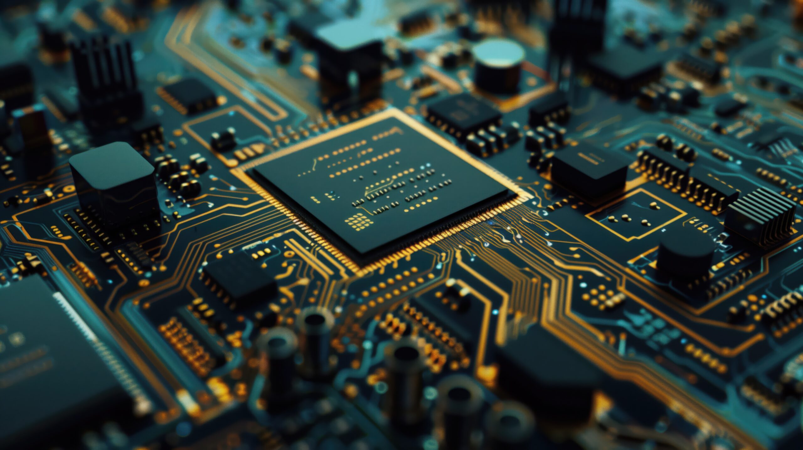
India’s semiconductor strategy is entering a new phase. On 15 July 2026, the Union Cabinet approved India Semiconductor Mission 2.0 (ISM 2.0) with a total budget outlay of ₹1,27,500 crore, significantly expanding the country’s policy support for semiconductor design and manufacturing.
The first phase of the India Semiconductor Mission largely concentrated on attracting semiconductor fabrication plants, Assembly, Testing, Marking and Packaging facilities and Outsourced Semiconductor Assembly and Test units. ISM 2.0 retains support for these activities but extends the policy focus to the wider supply chain required to operate semiconductor plants.
This includes semiconductor manufacturing machines, precision equipment, specialty materials, electronic-grade chemicals, industrial gases, chip design, research and development, advanced packaging and specialized workforce development. The official programme is structured around six pillars: design, machines and materials, additional fabs, ATMP and OSAT, research and development, and talent development.
The expanded scope creates potential opportunities for companies that may not manufacture semiconductor chips themselves but can supply products, technologies, utilities and services required by semiconductor facilities.
For businesses evaluating this sector, the critical question is therefore no longer limited to whether India will attract large fabs. It is whether a commercially viable domestic ecosystem can develop around those fabs and which Indian companies can realistically participate in it.
Semiconductor Policy is Becoming a Competition Between Ecosystems
The semiconductor industry has become a strategic priority for major economies because of its importance to electronics, telecommunications, automobiles, defence, artificial intelligence, industrial automation, energy systems and digital infrastructure.
Governments have adopted different combinations of direct grants, investment tax credits, concessional financing, state-backed equity, research funding, infrastructure support and workforce-development programmes.
The United States’ CHIPS programme was backed by US$52.7 billion, including US$39 billion administered as semiconductor manufacturing incentives. The US framework also includes an investment tax credit for qualifying semiconductor manufacturing and equipment facilities.
The European Chips Act was designed to mobilize more than €43 billion in policy-driven investment, alongside private investment, for manufacturing, research, pilot lines and supply-chain resilience.
Japan has similarly developed multi-year financial support mechanisms for advanced semiconductor manufacturing, artificial intelligence infrastructure and related supply-chain capabilities.
The global comparison is important because it shows that semiconductor competitiveness cannot be established by supporting a limited number of manufacturing plants in isolation. A sustainable semiconductor industry requires:
- Chip and system design capabilities
- Process equipment and precision components
- Wafers, substrates and packaging materials
- Ultra-high-purity gases and specialty chemicals
- Cleanrooms and specialised utility systems
- Assembly, testing and advanced packaging facilities
- Equipment maintenance and refurbishment capabilities
- Research institutions and specialised manpower
- Reliable domestic and export demand
What ISM 2.0 Covers
The official ISM 2.0 framework is organized around six interconnected pillars.
1. Semiconductor Design and Indian Intellectual Property
The programme aims to deepen India’s semiconductor design ecosystem and encourage the development of Indian intellectual property, chip designs and complete semiconductor systems.
Under the first phase, 24 semiconductor design projects received approval for financial support, while 105 start-ups and MSMEs obtained access to industry-standard Electronic Design Automation tools. These companies are working on applications including satellite communications, drones, surveillance systems, the Internet of Things, LED drivers, artificial intelligence, telecommunications equipment and smart meters.
Potential business areas include:
- Application-specific integrated circuits
- System-on-chip products
- Automotive and industrial semiconductors
- Power-management devices
- Telecommunications and networking chips
- Artificial intelligence accelerators
- LED drivers and display-related chips
- Smart meters and connected devices
- Verification and physical-design services
- Semiconductor intellectual-property blocks
Design businesses must, however, plan beyond the design stage. Prototyping, fabrication, testing, qualification, intellectual-property protection and customer adoption must be incorporated into the business and funding model.
2. Semiconductor Machines and Materials
The second pillar is one of the most significant additions under Semicon 2.0. It covers companies involved in the manufacturing and research and development of semiconductor machines, materials, chemicals and gases.
The Government has stated that this pillar is intended to create the foundation for sustainable semiconductor growth and strengthen India’s precision-manufacturing capabilities.
Reported policy details indicate that eligible new manufacturing units in semiconductor equipment, specialty chemicals, gases and materials may receive incentives of up to 30% of project cost. Detailed eligibility, approved expenditure and disbursement conditions will depend on the final scheme guidelines.
3. Additional Semiconductor Fabs
ISM 2.0 will continue to support silicon fabs, compound semiconductor fabs, discrete-component fabs and display fabs.
India’s first fab under the semiconductor programme is scheduled to be commissioned in 2028. The next phase seeks to attract additional global and domestic manufacturers while expanding the range of technologies manufactured in the country.
Reported incentive levels include support of up to 40% for silicon fabs and up to 35% for compound semiconductor, discrete and display fabs. These percentages should be read with the final notified rules and definitions.
4. Advanced Packaging and ATMP or OSAT Facilities
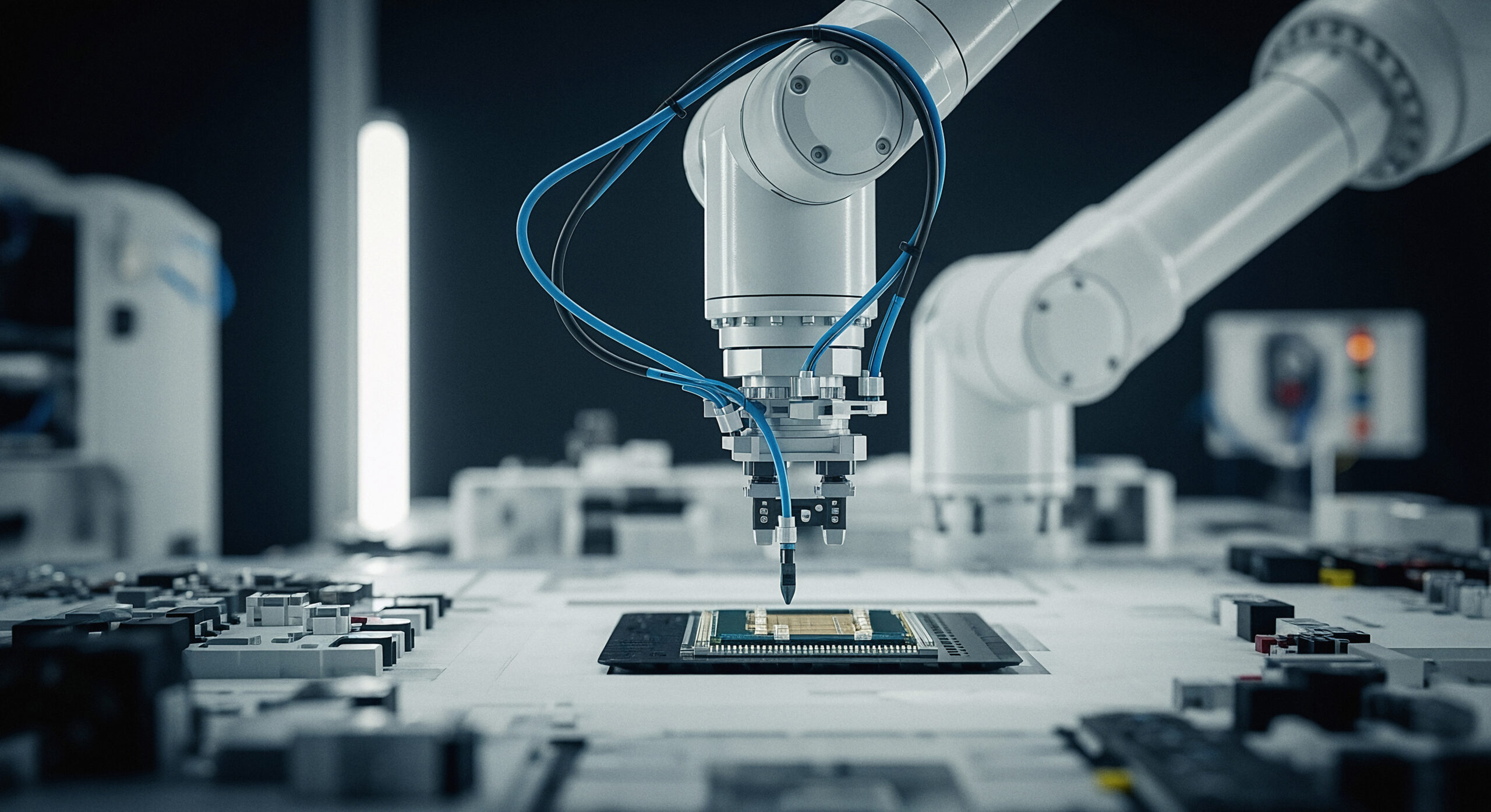
India has made relatively faster progress in semiconductor packaging than in front-end wafer fabrication. Semicon 2.0 seeks to attract more sophisticated ATMP and OSAT technologies, including advanced packaging.
Reported support levels include incentives of up to 35% for advanced packaging and up to 25% for conventional packaging, with states potentially providing additional support under their respective policies.
Opportunities may arise in:
- Conventional chip assembly and testing
- Flip-chip packaging
- Wafer-level packaging
- System-in-package products
- Multi-chip modules
- Heterogeneous integration
- Burn-in and reliability testing
- Failure analysis
- Packaging substrates and consumables
- Test and handling equipment
Advanced packaging is becoming increasingly important because improvements in semiconductor performance increasingly depend on integrating different dies, memory units, processors and specialised components within a single package.
5. Research and Development
India’s initial semiconductor manufacturing projects cover technology nodes ranging broadly from 28 nanometres to 110 nanometres. ISM 2.0 aims to support more advanced nodes and technologies through collaboration with research centres in India and overseas.
Potential areas include compound semiconductors, power electronics, advanced materials, semiconductor equipment, chip packaging, testing technologies and pilot manufacturing.
For commercial participants, research programmes will need clear arrangements covering intellectual-property ownership, technology transfer, pilot production and commercialisation.
6. Talent Development
The Government has reported that 315 universities are using modern Electronic Design Automation tools and approximately 68,000 students have already received relevant training. ISM 2.0 will extend the focus to cleanroom operations, fab construction and other specialized ecosystem capabilities.
This could create opportunities for technical institutions, training providers, semiconductor companies and equipment suppliers to develop practical programmes in design, process engineering, equipment maintenance, packaging, quality control, utilities and facility operations.
Progress Under the First Semiconductor Mission
ISM 2.0 is being introduced after India established an initial pipeline of semiconductor investments.
The Government has approved 12 semiconductor manufacturing projects with cumulative proposed investment exceeding ₹1.64 lakh crore. These comprise one silicon fab, one silicon carbide fab, an integrated gallium nitride Micro LED display fab and nine packaging units.
Micron, Kaynes and CG Semi had commenced commercial production by the time ISM 2.0 was approved, while another approved project was expected to begin production during 2026.
The Government reportedly expects ISM 2.0 to attract investment of approximately ₹4 lakh crore, generate semiconductor production of around ₹2 lakh crore and support exports of approximately ₹1 lakh crore over its six-year tenure. These are programme expectations rather than guaranteed outcomes.
The Central Shift: Localizing the Supply Chain Around Fabs
A semiconductor plant can create substantial industrial activity, but only when part of its procurement and supporting infrastructure is developed locally.
A fab that imports most of its equipment, chemicals, gases, parts, consumables and maintenance services may contribute to domestic chip production without developing a sufficiently deep local industrial base.
Industry participants have therefore emphasized that the implementation of ISM 2.0 should encourage semiconductor plants and their global suppliers to develop Indian vendors, localize appropriate manufacturing activities and establish long-term supply relationships.
The commercial opportunity extends across several categories.
Semiconductor Equipment and Precision Components
Semiconductor manufacturing requires highly specialised equipment for deposition, lithography, etching, cleaning, inspection, metrology, testing, wafer handling and packaging.
India is unlikely to manufacture every major semiconductor tool immediately. However, domestic opportunities can emerge in:
- Precision-machined parts
- Vacuum chambers and subsystems
- Pumps, valves and gas-delivery components
- Thermal-control equipment
- Robotic handling systems
- Electrical and control panels
- Automation systems
- Inspection equipment
- Cleanroom-compatible fixtures
- Equipment spares and consumables
- Calibration and maintenance services
Existing companies in aerospace, defence, pharmaceuticals, industrial automation and high-precision engineering may possess some relevant capabilities. Entry into semiconductor supply chains will nevertheless require higher standards of contamination control, traceability, repeatability and process documentation.
Specialty Materials and Chemicals
Semiconductor manufacturing uses an extensive range of chemicals and materials that must comply with stringent purity and consistency requirements.
Potential areas include:
- Electronic-grade solvents and cleaning agents
- Acids and process chemicals
- Photoresists and related materials
- Silicon wafers and specialised substrates
- Packaging compounds
- Bonding and encapsulation materials
- Thermal-management materials
- Filters and contamination-control consumables
- High-purity piping and storage systems
Conventional chemical-manufacturing capability does not automatically translate into semiconductor-grade capability. Purification technology, packaging, transportation, quality assurance and customer validation must be assessed separately.
Ultra-High-Purity and Specialty Gases
Semiconductor fabs require nitrogen, oxygen, argon, hydrogen and several specialised process gases in highly controlled purity levels.
INOX Air Products has been developing a ₹500 crore electronic specialty-gas hub in Dholera, Gujarat, intended to support the semiconductor ecosystem developing around the Tata Electronics fab and other regional users. The planned facility is expected to supply ultra-high-purity bulk and specialty gases, while more complex products may be introduced as domestic demand and technology partnerships develop.
This example illustrates how an anchor fab can generate investment in adjacent infrastructure. It also demonstrates that localisation may occur in stages. A supplier may initially import certain gases while developing storage, distribution, quality-control and customer-service capabilities, followed by local production as demand becomes sufficiently large.
Cleanrooms, Utilities and Environmental Infrastructure
Semiconductor plants require specialised supporting infrastructure, including:
- Cleanrooms and contamination-control systems
- Ultra-pure water generation
- Wastewater recycling and treatment
- Chemical-management systems
- Hazardous-waste treatment
- Continuous and high-quality power supply
- Backup and emergency systems
- Process-gas storage and distribution
- Vibration-control systems
- Facility monitoring and automation
Engineering, construction and utility companies can participate in these areas, but semiconductor projects require specialised design standards, validation procedures and operating capabilities.
Refurbished Semiconductor Equipment: An Emerging Opportunity
A further opportunity identified by industry participants is the refurbishment of semiconductor manufacturing equipment.
Fabs do not necessarily purchase every tool as new equipment. Depending on the technology node, process requirement, production economics and equipment condition, refurbished machinery can be used for selected applications. Industry participants cited in the recent report estimated that refurbished tools may account for approximately 20% to 30% of equipment in some fab configurations.
Developing a domestic refurbishment ecosystem could create opportunities in:
- Used-equipment sourcing
- Equipment inspection and certification
- Refurbishment and retrofitting
- Replacement-part manufacturing
- Calibration and process validation
- Software and control-system upgrades
- Installation and commissioning
- Annual maintenance and field service
- Operator and maintenance training
This segment is relevant because refurbished tools may reduce capital costs and shorten procurement lead times, particularly for mature-node fabs, research facilities, pilot lines and training centres.
However, used-equipment decisions require disciplined technical evaluation. Factors such as OEM support, remaining useful life, spare-part availability, process compatibility, warranty, export restrictions and future upgrade capability must be examined before procurement. Government norms have also historically imposed conditions relating to OEM support and remaining equipment life for eligible refurbished tools.
India’s opportunity is therefore not merely to import used machinery. It is to develop local engineering, refurbishment, spare-parts and lifecycle-support capabilities around such equipment.
Seoul Semiconductor’s Reported India Plans: An Early Investor Signal
The reported interest of South Korea-based Seoul Semiconductor provides an example of how ISM 2.0 may influence investment decisions.
Seoul Semiconductor develops LED and optical semiconductor technologies for automotive, display, lighting and industrial applications.
Recent reports indicate that the company is exploring a manufacturing facility in India and has been in discussions with the governments of Tamil Nadu, Karnataka and Gujarat. Its present manufacturing operations are located in South Korea, China and Vietnam.
The company is reportedly considering establishing its first Indian base through a packaging or assembly facility before evaluating a larger manufacturing presence. Depending on the final project configuration, it may examine incentives for LED wafer fabrication, advanced packaging or conventional packaging.
No final location, investment amount, scheme application or binding project commitment had been publicly announced when the reports were published. The relevant incentive eligibility will also depend on the detailed ISM 2.0 guidelines.
The development is nevertheless commercially relevant for three reasons.
- It indicates that the policy is attracting interest from companies outside conventional silicon semiconductor manufacturing.
- It highlights the potential role of optoelectronics, LEDs, displays and specialised semiconductor packaging within India’s emerging ecosystem.
- Competition between states will increasingly depend on more than fiscal incentives. Utility readiness, electronics demand, supplier availability, logistics, manpower, land, implementation support and proximity to customers will influence actual location decisions.
Opportunities for Existing Indian Companies
ISM 2.0 could create entry opportunities for businesses with capabilities in adjacent industries.
1. Precision Engineering Companies
Manufacturers serving aerospace, defence, pharmaceuticals, automotive and industrial-equipment markets may evaluate semiconductor-compatible components, chambers, fixtures, fluid-control systems and equipment subsystems.
2. Chemical and Gas Manufacturers
Companies with experience in specialty chemicals, industrial gases, purification and process materials can evaluate semiconductor-grade product lines. Such entry will normally require technology upgrades, quality systems, specialised packaging and customer qualification.
3. Electronics and Automation Businesses
Companies operating in robotics, sensors, machine vision, control systems, power electronics, test equipment and factory automation can assess products and services required by fabs, packaging facilities and semiconductor laboratories.
4. Packaging and Testing Businesses
Electronics manufacturing and testing companies may evaluate ATMP, OSAT, reliability-testing, burn-in and specialized packaging opportunities. The selected technology must be aligned with identified customer requirements rather than based solely on available incentives.
5. Infrastructure and Engineering Companies
Companies in cleanrooms, water treatment, waste management, electrical infrastructure, process piping, gas handling and facility operations may participate in semiconductor-support infrastructure.
6. Training and Technical Institutions
Institutions can develop programmes in chip design, semiconductor processes, cleanroom practices, equipment maintenance, packaging and facility engineering. Training programmes must remain aligned with actual equipment, production processes and employer requirements.
| Evaluating a Business Opportunity Under ISM 2.0? Before committing capital to semiconductor design, equipment, specialty materials, electronic-grade chemicals, gases, packaging, testing or supporting infrastructure, businesses should evaluate the addressable market, customer requirements, technology access, policy eligibility, location suitability, implementation risks and long-term financial viability. Hmsa Consultancy Services assists businesses in evaluating semiconductor-linked opportunities through feasibility studies, detailed project reports, market assessments, business planning, incentive assessment and financial evaluation aligned with actual investment decisions. Share your proposed project requirements with us here. |
Conclusion
ISM 2.0 represents a material expansion of India’s semiconductor strategy. The programme is no longer centred only on attracting fabs and assembly facilities. It seeks to develop capabilities in design, equipment, materials, chemicals, gases, advanced packaging, research and specialised manpower.
The reported interest from companies such as Seoul Semiconductor and investments such as the electronic specialty-gas hub in Dholera indicate that semiconductor activity can begin generating investments across the supporting supply chain.
The larger opportunity may therefore extend to precision manufacturers, chemical companies, industrial-gas suppliers, engineering businesses, automation companies, infrastructure providers, electronics firms and technical institutions.
However, semiconductor-linked investment remains complex. Successful entry will require a clearly defined position in the value chain, access to technology, customer validation, appropriate project scale, infrastructure readiness and realistic financial planning.
ISM 2.0 can improve the investment environment. Commercial viability will ultimately depend on whether individual businesses can develop competitive products, meet semiconductor-grade standards and secure a sustainable route to customers.
Reference: Economic Times